
Let’s say you are given an assignment that includes several blocks used in one area with a clear restriction in one dimension. This is common in the development of a memory product when the memory core defines the periphery limitations.
There are several factors you need to know to thoroughly plan out the area and I want to focus on one aspect that involves both area and general floor planning.
In the early stages of planning can help you determine the approximate aspect ratio of each sub-block within your assigned area.
This method was originally developed using little or no add ons, relying on the ability of a solo custom layout designer using the base layout tool from Cadence.
An ideal application for this method is when an entire side of a memory array core is reserved for the layout of special power supply circuits, but this area estimating method can be used for any functional block with one dimension restricted.
In the memory array example, you know the total width of the array core but the extension from the array for your assignment is initially unknown, it’s one of your objectives to take up as little space as possible to save chip size.
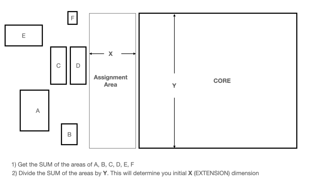
STEP 1: Get an estimation of the AREA of each sub-block.
The more accurate your estimate the closer you will be to a real number, and don’t be too concerned about the X and Y dimension yet, just get an area. Considering this in an initial estimate, you can “ball park” estimate certain details in effort to save time, especially if the design stage is not well simulated at the time you perform this planning.
This is not the focus of this article but you can estimate area using a number of strategies, nowadays, one of the most common is to generate the P-Cells from the schematic. Another way is to use a ready library of scratch cells (your personal customized layout parts and device bin) to approximate the requirements of each schematic. Those who are more abstract in their thinking, can count the transistors and know an approximate space required. Busing and power area always a consideration and how much you can layout underneath them.
STEP 2: With an AREA estimation for each sub-block, do these calculations:
- Add all the estimated areas of each sub-block together, this equals your Total Area.
- Divide the Total Area by the dimension of the array/core (or whatever measurement is the defining the limit for your assigned area). This quotient will give you an EXTENSION dimension from the array. For now, let’s call the Extension “X”.
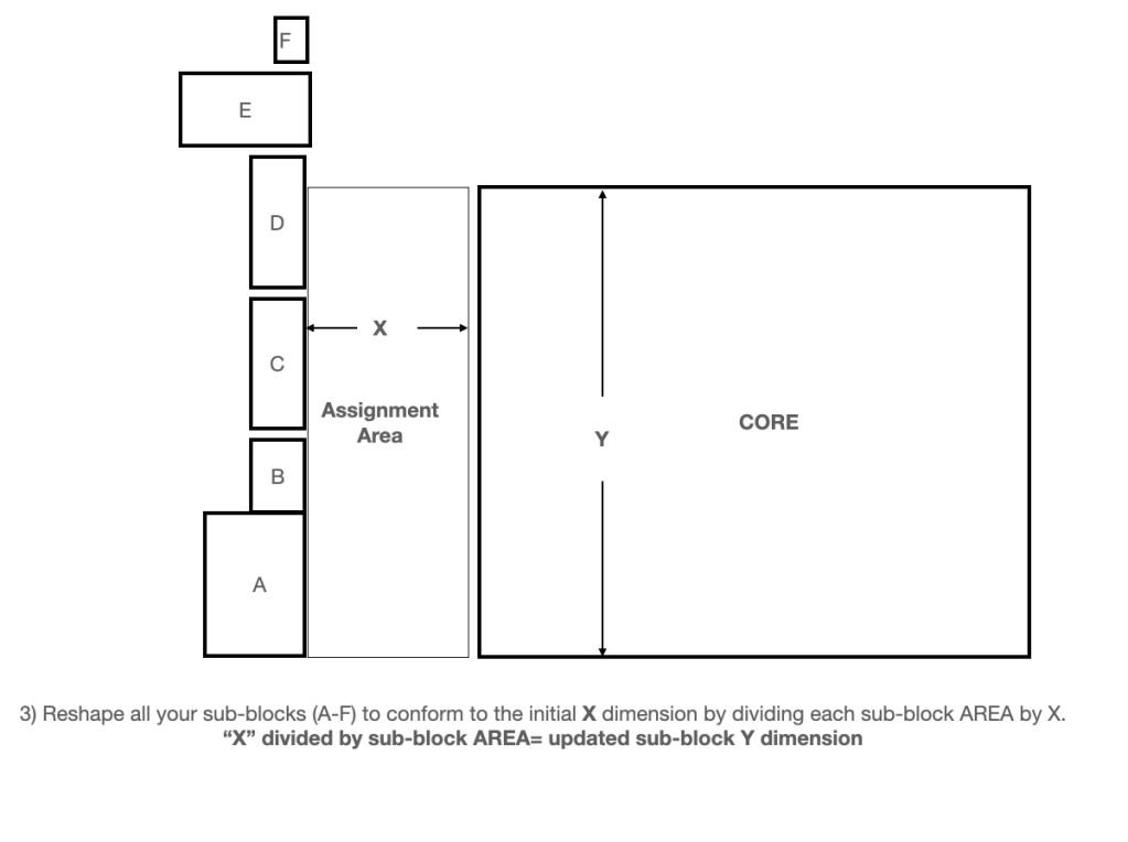
- Use this “X” to adjust all of your sub-blocks. In other words, sub-block Area divided by “X” = the new sub-block “Y” dimension.
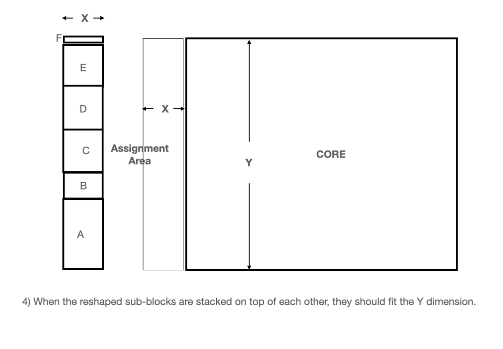
At this point you will have your initial targets for each sub-block for both X and Y dimension and all the sub-blocks should stack neatly into your assigned space.
And can begin to refine or define the floorplan for each block.
See below for a graphic explanation:

See the reshaped sub-blocks below and the adjusted X dimension based on the calculation in Illustration 2:
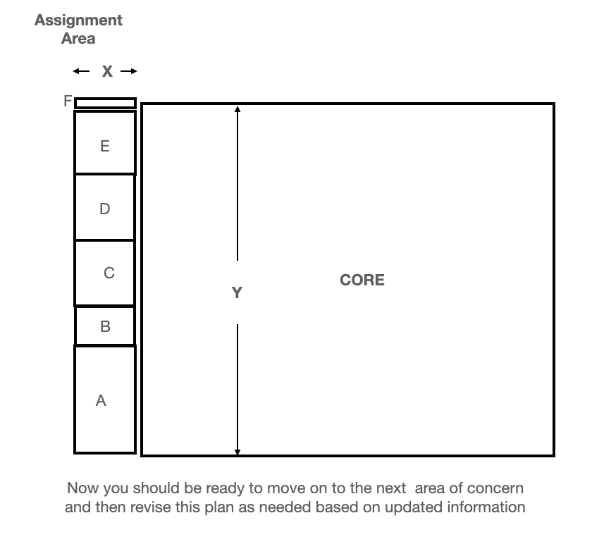
Some of the benefits of this kind of planning allows for clear partitioning of work areas and easy mobility in positioning. Global details should be defined by the lead layout to ensure consistency across the area while meeting global considerations, connectivity and boundary conditions.

Please like, share, follow, and/or comment . Glad to help with any of your non-NDA violating concerns.
CKY
***
Copyright © 2023 ChallenYee / ICLayout.blog Some Rights Reserved

Leave a comment