

In your planning of how to organize a layout and its subcells, there are several considerations in creating a manageable hierarchy. One thing to look out for are transmission gates (XFR gates).
A general principle is an inverter is best to drive lines and XFR gates are not. XFR gates are bad drivers, simply, because (drum roll…) they are not drivers.
In terms of parasitics, XFR gates are like the guy who comes to lunch who doesn’t pay his bill because he never brings a wallet (and then makes you, the driver, pay). 😉 (I hope you get the joke).
NANDS and NORS are also in the general category of drivers because they can regenerate a signal with VDD or GND, but inverters are the best because they can be most easily adjusted on the schematic and layout side and have the least amount of secondary effects on the floorplan and the device sizes in the schematic (i.e. how many drivers to the inputs need to be considered when there is a size change).
Depending on how you separate the layout, that will have an effect on how far certain signals need to be driven and that may or may not fall within the criteria of the circuit engineer’s timing margin. A circuit designer should highlight nodes that require special attention, sensitive, noise intolerant nodes, heavily loaded nodes, that sort of thing, to make sure those devices or nets are carefully layed out. If not, you should ask when dealing with an unfamiliar circuit.
As a layout designer, sharing some of that circuit engineer mentality will help ensure that you can look at the schematic with your own sense of discernment in the collaboration process.
Another consideration are the LATCHES which are often closely associated with XFR gates. XFR gates often have a drain connected to the storage side of a latch, see ILL. 1 junction between x2 – drain and w1 – output.
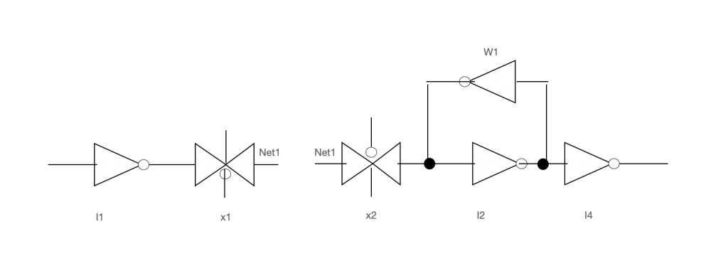
In a random logic circuit, you often see several latches and input of each latch (i2/w1) is preceded by an XFR gate (x2). In general, you want to keep this latch together with the XFR since the XFR is not designed to drive and the “memory” node (x2 to w2 junction) of a latch is subject to undesired flipping from net noise if the net is too exposed (i.e. too long or too adversely noise coupled).
If an XFR gate (x1) drives another XFR gate (x2), you may be able to separate those, but consideration must be given to the drive strength of the XFR gate and the buffer driving it.
If the distance between XFR gates becomes “too long” the circuit designer needs to know, so he can either so “NO”, “OK”, or “OK, but I need to adjust the sizes”. If unsure how long is too long, ask the circuit designer.
A large XFR gate is suspect without an adequate driver/buffer in front of it to drive the signal through the little parasitical monster. A rough rule of thumb seems to be a driver of about the same size as the XFR gate. Too many increased sized drivers equals more power usage also, like in a high speed path with many bits, so keeping driver sizes small is better when possible.
***
I like coffee and maybe you do also, but if you are experiencing headaches, joint pain or soreness, it may be the result of too much caffeine. Try backing off for a few days and drink more water see how it goes.

Feel free to Like, Share, Follow, and Comment
CKY
***
Copyright © 2023 Challen Yee / ICLayout.blog Some Rights Reserved

Leave a comment