IC Layout

Integrated Circuit Layout Design

Challen Yee AMS Layout Engineer

ICL 23.10 Quick tip: Read Bus Capacitance Reduction

I ran across this situation when I was drawing the high speed read data path for a special memory and capacitance of a shared data bus became an issue. On certain schemes, there may be multiple transmission gates (XFRs) connected to the same bus line, hence, the cumulative drain capacitance caused some concern on the SIMs.

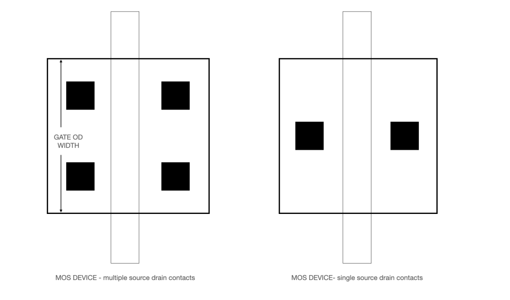
The consideration is if you need to reduce capacitance, and the metal bus is already drawn to its minimum width and optimal spacing, and decoupled from other noise or other voltage nets. In order to further decrease capacitance, you may consider reducing the number of contacts on the source and drain of the XFRs.

You may see fit to reduce the number of contacts, since every contact within themselves adds capacitance.

Of course, you need to consider the DRC rules, however, it is recommended the reduction in capacitance needs to be weighed vs added resistance of decreasing the number of contacts.

ILLUSTRATION 1

For an eye exercise, you can focus on your thumb moving it near and to the fullest extent of your arm and around from periphery to periphery to refresh some blood circulation to your eyes.

Feel free to Like, Share, Follow, and Comment

CKY

***

Copyright © 2023 Challen Yee / ICLayout.blog  Some Rights Reserved

Disclaimers

2 responses to “ICL 23.10 Quick tip: Read Bus Capacitance Reduction”

  1. Hi CKY,
    For high speed signals at lower nodes especially in FinFET, the tradeoff between the parasitic capacitance and resistance is a tough call to make. For eg: Double gate contact is a mandatory requirement for very high speed signals. I would like to hear your suggestions on it. I also have a request. Please do cover a post on ESD, chip level Floorplan and area allocation/optimization, Bump placement, Macro placement etc. on your subsequent posts.

    Liked by 1 person

    1. Hi ARK, That does sound like a tough call. I can see how the oxide thicknesses demanding tall and steep chimneys.One thing the layout designer can control is the unnecessary baggage (antennas), once all the line width and pitch are optimized. You will want to look at all your coupling (neighboring nets) to help reduce the CAP in each situation. May require refloorplaning or relocating pins or metal routing to reduce coupling. Always be mindful of voltage difference. . I have thought about writing about package and pinout, ESD, more on floor planning, so on and so forth. At least I’ll know I have one interested reader 😉

      Liked by 1 person

Leave a reply to ark Cancel reply