
Philosophy related to the Project Custom Reference Library (PCRL).
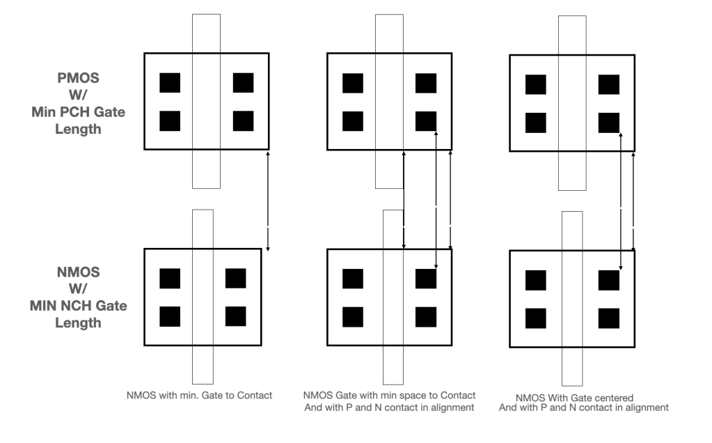
One of the issues one runs into with many CMOS logic technologies is the asymmetry of default or minimum P and N channel gate lengths.
If you’ve run into this problem, when all the geometries are drawn, the NChannels “pack in” tighter than the PChannels.
What you end up with is this constant shift in alignment between the PCH and NCH and more often than not, source and drain do not align equally to the left or right borders of the cell in a given string of devices, so when if the MOS devices are arrayed there is a large void space made possible by the larger length PMOS.
If identical subcells are placed together in a reflected manner, with the intention of sharing contacts, the contacts are not in alignment on the X-Axis.
There’s not just one way to address this problem. After all, it’s custom layout.
In one solution, the source contacts can always be stretched to be in alignment so that identical cells can be reflected and aligned with overlapping contacts, which can save space.
In methodology, if you can rely on certain standards built into the layout, sometimes those standards are able to be globally manipulated with only a reasonable backlash.
This issue can be addressed with PCELLs also, by editing the parameters that control the gate to source contact spacing.
Just as a matter of discussion, this brings to mind a couple of ideas that may have some influence, albeit minor, in how you think about the layout.
The contact to gate spacing could be adjusted so that the contacts remain in alignment between the PMOS and NMOS. You might argue, “Doesn’t this add more capacitance and resistance by moving the contact further away from the Ngate?”
You would be correct, but the difference is not as large or significant as you may think, especially knowing that the resistance across the gate is substantial compared the the OD resistance. Furthermore, if there were other good reasons to prepare the layout with P and N contacts in alignment, which may be desirable in digital layout with analog or matching OD and poly topography considerations, the added diffusion area may be quite insignificant.
In terms of layout discipline and methodology, these reference parameters should be maintained in the development of subcells and only in extreme situations, like pitch layout or cell layout, should this artificial extension built into the reference layout be violated. This is a consistency that may be relied upon in certain R/D scenarios where a gate length can be biased for effect with minimal disruption to the layout.
***
If you have digestion problems and GERD, you might benefit from a tablespoon of vinegar in a cup of water. GERD is often a case of NOT ENOUGH stomach acid, not too much acid.
Feel free to Like, Share, Follow, and Comment
Could be a Greek philosopher 😉
CKY
***
Copyright © 2023 Challen Yee / ICLayout.blog Some Rights Reserved

Leave a reply to ICL WW-23.02 Weekly Wrap for 11-13 thru 11-17-23 – IC Layout Cancel reply