

How many times have you asked yourself while running ESD or antenna verification why certain nets need a diode and then it can be difficult to figure out how to implement the fix?
Here are some criteria that if the error tolerances are exceeded, you should get an error.
(This is off the top of my head, so if you can think of some others error conditions, I’d welcome you comments)
- No Source Drain connected to net with a gate device connected to it.
- Too much antenna exposure (ability to accumulate electrostatic charges) to a gate before the entire net is connected during manufacturing.
- Not enough Source Drain connected to net (the proportion exceeds tolerance).
- In other words, during manufacturing or operation, the possibility of a gate device becoming “burnt toast” exceeds the desired criteria to yield properly (ok, “burnt toast” it’s not a technical term, but you get the idea I hope).
The essential principle is, if these violations are not fixed, the typical result is the likelihood that a gate (or gate oxide) or blow up when too much static charge tries to discharge through the gate.
It may be that not all these gates would die if they are not fixed, but one gate dies and the yield will decrease and that’s never good when it’s the result of something that is caught with a DRC and should be fixed.
There are a couple of ways these antenna or ESD errors are commonly fixed, some require an alteration to the existing layout and some can only be fixed by adding a diode, or a small patch of OD (the opposite of a guard ring tap) to allow a safe discharge path for static charges. Adding a diode that is from a PCELL or library will require a schematic change, though in some cases not. In general the schematic change is a good idea so that the Circuit Engineer is aware of the added device(s) on that net.
Methods/Scenarios
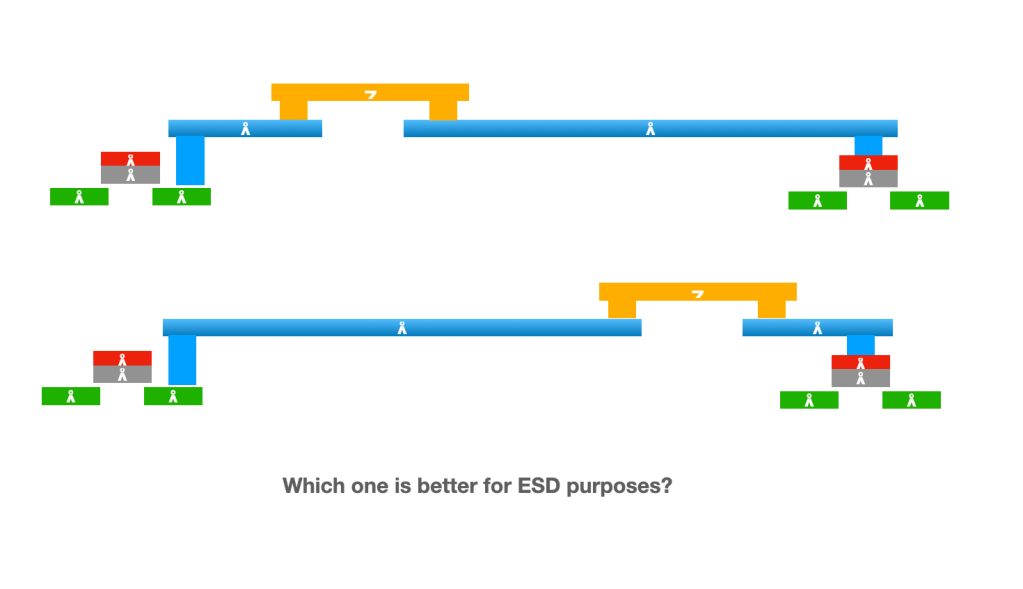
- Decrease the amount of metal connected directly to a gate before the top layer metal is manufactured for that net. For example, if you use a multi metal layer process, but the net only runs in M1, then you could cut the M1 near the gate in question and create a M2 bridge. The idea is, the gate will only see a very small charge until the entire net is connected, allowing for any static build up to discharge through the drain connection.
- Furthermore, if the net of the problem gate is connected to, for example, up to M3, then you need to evaluate the total M1 and M2 connected to the gate BEFORE it sees a M3. Too much lower level metals will store charges without a proper means of discharge.
- If the error still persist in scenario #1, then a diode needs to be placed, near the gate and connected to the same M1 that is connected to the gate.
- If it’s not possible to place a diode, then metal width reductions or possible a device size increase could top the balance of the error threshold. Usually we do not alter gate sizes in a normal scenario though because, it requires a schematic change and the device size is usually optimum for that given net. If this can fix the problem, however, you need to collaborate with you circuit engineer. WARNING, any time you change the characteristics of a net, you need to assess that it for its analog/matching specs designed into it.
- You may also want to look at excessive vias, which are acting like little capacitors to blow up your gate also.
- Pull back “antenna” or unused metal interconnect (However, be careful not to destroy matched nets/busses by making them unequal in the process).
- When placing diodes, place them close to the device in question. Placing a diode in another neighborhood makes it an ineffective fire fighter to cool down the pre- burnt toast condition.
- Some PCELL or standard diodes are large than the minimum size possible, so you can explore the possibility of creating your own diode that takes less space if space is too tight. As long as it passes DRC, the OD area should be adequate. Warning: Any deviation from standard methodology should be discussed with your resident technologist and/or project leader.
- Not as obvious is when even the “top metal” of the net or ANY metal net on that circuit is considered too large and needs to be broken or a diode added to keep accumulated charges within spec, to avoid the hypothetical TSUNAMI of electrostatic charge from careening into the poor little gate and turning it into burnt toast.
- Even more not as obvious will be the effect of unrelated nets. If this is the case, you may need to reduce the edge (fringe) or area capacitance associated with the net connected to the gate, as long as you are not destroying the necessary decoupling and shielding considerations given to that net.
This should be enough for you to chew on for now.
I hope the injection of non technical terms is not too distracting for you.
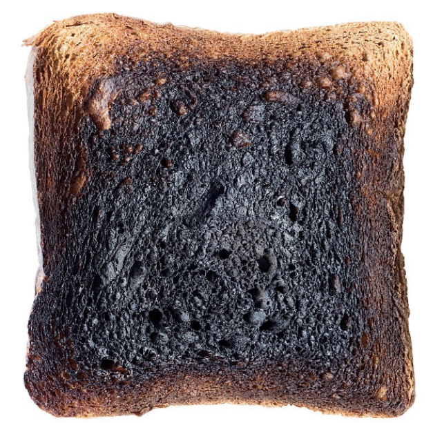
Image source: istockphoto.com
***
Feel free to Like, Share, Follow, and Comment
CKY
***
Copyright © 2023 Challen Yee / ICLayout.blog Some Rights Reserved

Leave a reply to ICL WW-23.03 Weekly Wrap for 11-27 thru 11-30 – IC Layout Cancel reply